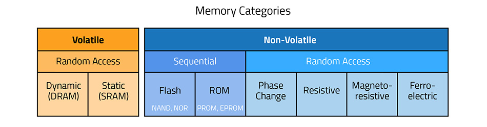
Memory technologies are often categorized by how data is stored (volatile or non-volatile) and accessed (random or sequential). In terms of function, there are two broad classes of memory: primary (main memory, or memory), which is the active type that works on data, and secondary (data storage), which provides long-term storage.
For memory, speed is critical because it holds the data currently being used and/or changed. Imagine your favorite video game pausing every time you make a move or missing a turn when your smartphone’s GPS app can’t reroute directions in time. Cache, a subset of main memory, has the highest speed requirement as it stores instructions awaiting execution. DRAM is the most common technology used for main memory because of its speed and ability to individually access the smallest unit of data, which are key requirements.
For storage, where data like photos and documents are kept, data integrity and storage longevity are far more important than speed. Today, capacity for a storage device can be in the terabyte range (that’s a thousand gigabytes or one million million or 1012 bytes). Flash memory is the primary type used for storage. Here, capacity to hold data and cost-efficient manufacturing are important, given the ever-growing demand to be able to retain large volumes of data.
DRAM
For main memory, DRAM (dynamic random access memory) is the current standard. DRAM is a type of volatile memory, meaning it requires power to retain data. “Dynamic” refers to the slow discharge of the capacitor (data leakage), where the charge periodically needs to be refreshed to retain the data. This is less than ideal as it consumes extra power and requires high endurance (ability to read and write many times). “Random access” means it takes the same amount of time to reach any memory address. This provides efficient data access compared to the slower sequential (in the order data was stored) access of NAND flash and other storage-class technologies. Another speed advantage is that DRAM is bit-alterable, where new data can directly overwrite existing stored information (no erase step needed). DRAM is also bit-addressable, allowing access to individual bits of data and not just larger blocks (often called “page read”), which is important for main memory.
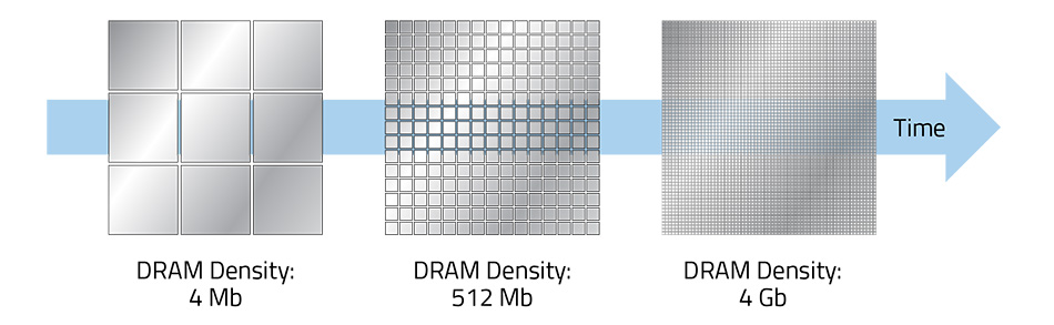
DRAM’s tiny one capacitor-one transistor design makes it ideal for packing numerous memory cells into a small area to achieve high density and high storage capacity. In fact, billions of DRAM cells can be squeezed onto a single memory chip. For years, speed, capacity, and power improvements were made by shrinking device features using single-pass lithography. To continue scaling, multiple patterning – which involves additional lithography passes and sequences of deposition and etch – now compensates for lithography resolution limitations. Even so, DRAM capacitors can be made only so small and still be able to store a charge (data). Also, the smaller the device, the more vulnerable it is to electrical leakage.
Flash Memory
Flash memory is a type of non-volatile memory (data is retained after the power is turned off) used for data storage. The two types, NOR and NAND, get their names from the type of logic gate used in the cell. NOR flash reads and writes data one word (all the cells in one memory chip) or byte at a time, which allows random access to each address. NAND flash manages larger amounts of data and is faster than NOR, but existing data must first be erased before new data can be stored. Neither is as fast as DRAM, nor are they bit-addressable or bit-alterable, so they do not provide the performance generally required for main memory.
NAND is a smaller chip than NOR, so it can achieve higher density, and it is less costly to manufacture. Thus, NAND flash has become the mainstay for high-capacity storage-class memory, where it’s used in memory cards, USB drives, and solid-state drives for every day products like computers, digital cameras, smartphones, and other mobile devices. While DRAM is still advancing planar (horizontal) scaling to increase capacity, NAND has achieved density scaling by going vertical as in 3D NAND. Here, memory cells are added by going up instead of out to the side, where space on the wafer and inability to further shrink device features limit density. Of course, there was nothing simple about designing a completely new architecture that involved flipping the cells on their side or developing the new fabrication processes needed to manufacture them. For more on vertical scaling and 3D NAND, take a look at our Tech Brief, Memory “Grows Up” with 3D NAND.

New Memory
Although DRAM likely has a couple more generations of improvements to go, several alternatives are being explored. For example, the industry is discussing possible future 3D architectures. Likewise, a number of disruptive memory technologies are in development that target storage-class applications. Stay tuned for our upcoming Tech Brief, “ABCs of New Memory,” which will explore these new memory types – how they work, their applications, and the challenges ahead in developing these promising technologies.
Meanwhile, we hope this brief review of memory types and applications has been helpful in clarifying the various distinctions. The next time you read about memory that is volatile or non-volatile, uses random access or sequential read, or involves some other category, you’ll have a better idea of its classification and likely applications – provided you can remember all this…
Courtesy of Semiconductor Engineering